
China Strengthens Integrated Circuit Layout Protection as Semiconductor IP Rules Are Modernized
China has substantially revised its legal framework for protecting integrated circuit layout designs. The changes update a system that had remained largely unchanged since 2001 and align it more closely with current semiconductor technology, increasingly complex chip designs and the commercial importance of intellectual property.
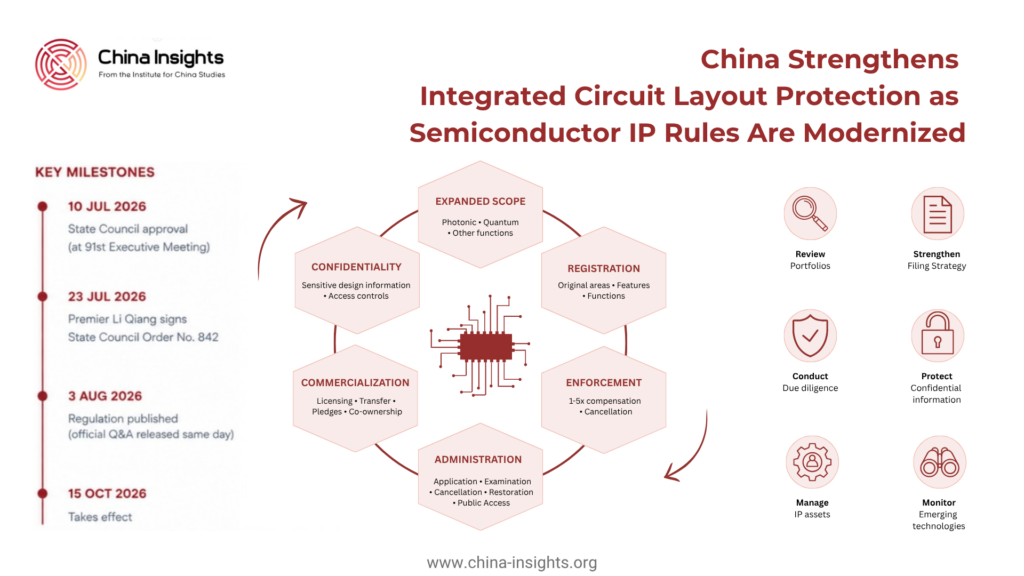
The State Council approved the revised Regulation on the Protection of Integrated Circuit Layout-Designs (《集成电路布图设计保护条例》) at its 91st Executive Meeting on 10 July 2026. Premier Li Qiang signed State Council Order No. 842 on 23 July 2026. The revised regulation was published on 3 August and will take effect on 15 October 2026. The Ministry of Justice (MOJ) and China National Intellectual Property Administration (CNIPA) published their official Q&A on the revision on the same day.
Executive summary
- Protection is extended to layout designs for integrated photonic, quantum and other functional integrated circuits.
- Applicants must now identify the specific original design areas, design features and corresponding functions supporting protection.
- Third parties gain a formal mechanism to request cancellation of registrations that do not meet statutory requirements.
- The framework introduces punitive damages of one to five times the otherwise determined compensation in serious cases of intentional infringement.
- Procedures for application, examination, cancellation, restoration of rights and public access have been strengthened.
- Confidentiality protections have been reinforced because registration materials may contain commercially sensitive design information.
- The changes increase the importance of systematic layout-design registration and IP management for semiconductor companies operating in China.
Protection expands beyond traditional semiconductor layouts
The most significant substantive change is the expansion of the technology covered. The revised regulation removes the previous limitation reflected in the definition of integrated circuits and explicitly provides that layout designs for integrated circuits with photonic, quantum and other functions may receive protection.
This matters because semiconductor innovation is increasingly moving beyond conventional architectures. Photonic integration and quantum technologies are developing alongside established semiconductor technologies. The revised framework gives companies a clearer route to protect layout-related intellectual property in emerging technology fields.
For businesses, the change reduces the risk that new chip architectures will develop faster than the IP framework protecting them. It also signals that China’s layout-design protection system is intended to accommodate future technology development rather than remain limited to the technologies prevalent when the original regulation was introduced.
Registration becomes more precise
The revised regulation introduces more detailed requirements for registration materials. Applications must include copies or drawings containing the necessary information to clearly show the original parts of the layout design. Applicants must also provide an originality statement identifying the design areas, design features and corresponding functions that are considered original.
This changes the practical significance of registration. Previously, the framework required submission of copies or drawings but provided less detail on how these materials should demonstrate the protected scope. The revised rules are intended to make the protected elements more identifiable and therefore easier to assess in potential disputes.
For semiconductor companies, registration should therefore become a more deliberate IP-management exercise. Design teams and legal teams will need to work together to identify commercially important original elements before filing.
Infringement protection becomes stronger
The revised regulation strengthens remedies for serious infringement. Where an infringement is intentional and the circumstances are serious, compensation may be increased to between one and five times the amount otherwise determined.
This is a material change in the risk profile for companies dealing with protected layouts. The introduction of punitive damages creates a stronger financial deterrent against deliberate copying and commercial use of protected designs.
For rights holders, the change potentially increases the economic value of effective registration. For companies using third-party chip designs, it also increases the importance of conducting IP due diligence and maintaining evidence that products and design activities do not infringe protected layouts.
Third-party cancellation becomes easier
The revised regulation also changes the cancellation mechanism. Under the previous framework, the relevant cancellation process was principally initiated by the competent authority itself. The revised regulation allows any person who believes that a registration does not comply with the regulation to request its cancellation.
This creates a more accessible mechanism for challenging registrations. It may become particularly relevant where competing companies believe that a registered layout does not meet the required conditions or where registration information is disputed.
The change strengthens the administrative review dimension of the system. Companies should therefore assess not only their own registrations but also potentially relevant third-party rights when entering disputes, transactions or technology partnerships.
Rights recovery and procedural protection improve
The revision also improves several procedural elements. These include more detailed rules covering rejection, cancellation, restoration of rights and other stages of the registration process. The regulation establishes a clearer procedural framework than the previous version.
For businesses, this is important because IP value depends not only on substantive rights but also on the ability to maintain those rights through administrative procedures. Clearer restoration mechanisms can reduce the commercial consequences of procedural failures where the relevant statutory conditions are met.
The broader direction is toward a more mature IP administration system. Companies will need stronger internal processes for filing deadlines, documentation and monitoring of registration status.
Confidentiality becomes a greater compliance issue
The revised rules recognize a potential tension between stronger disclosure requirements and the commercial sensitivity of chip layouts. Registration materials must contain enough information to establish originality, but those materials can also contain valuable technical information.
The regulation therefore strengthens confidentiality protections. Electronic versions of layout-design copies or drawings generally cannot be accessed or copied by third parties except where government authorities require access for legally defined functions. It also establishes responsibilities for officials, relevant personnel and patent agencies handling unpublished information.
This is relevant for companies with highly sensitive chip designs. Internal controls around registration documents, external agents and disclosure procedures will become increasingly important.
Commercialization and ownership are better defined
The revised framework also strengthens provisions relating to the use and commercialization of layout-design rights. It provides clearer rules concerning transfer, licensing, pledges, co-ownership and remuneration arrangements.
This can make layout-design rights more usable as commercial assets. Companies can increasingly treat protected layouts as part of broader IP portfolios rather than only as defensive rights.
For investors and technology partners, this should improve the ability to assess ownership, licensing and transaction risks associated with chip-related IP.
Implications for foreign semiconductor companies
The revised framework continues to provide protection for qualifying foreign-created layout designs. Foreign individuals, companies and other organisations can obtain protection where their designs are first commercially exploited in China or where the relevant international arrangements provide for protection.
This is relevant for multinational semiconductor companies conducting design, manufacturing, licensing or commercial activities in China. The revised rules do not eliminate the need for jurisdiction-specific IP strategies, but they provide a more developed domestic framework for protecting layout-design rights.
What this means for business
- Review layout-design portfolios: Existing registrations should be assessed against the revised requirements before the new rules take effect.
- Strengthen filing strategies: Companies should clearly identify commercially important original design elements in registration materials.
- Increase IP due diligence: The possibility of third-party cancellation and higher infringement damages raises the importance of checking competing rights.
- Protect confidential information: Registration processes should be integrated with technical-information security and disclosure controls.
- Treat layout designs as commercial assets: Licensing, transfer, pledging and co-ownership rules create greater scope for active IP management.
- Monitor emerging technologies: Companies developing photonic, quantum or other advanced integrated circuits should assess the expanded protection framework.
Sources
https://www.gov.cn/zhengce/202608/content_7077409.htm
https://www.cnipa.gov.cn/art/2026/8/3/art_106_207524.html
https://www.cnipa.gov.cn/art/2026/8/3/art_66_207423.html
https://www.cnipa.gov.cn/art/2026/8/3/art_66_207422.html
Author
Dr. Richard van Ostende

Related Articles